
The gap waveguide is built up of two parts: a structured metal surface and a flat metal surface being placed in close proximity to one another. The structured surface is characterized by pins forming a barrier preventing the electromagnetic waves from propagating in undesired directions, resulting in signal losses as low as for rectangular waveguides.
可以提供26.5~110GHz的GAP轉接波導,產品聯系:sales@gamtic.com,021-5197 0121.
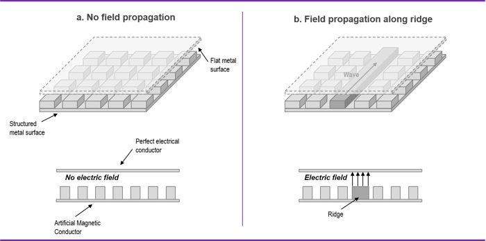
The gap waveguide is built up of two parts: a structured metal surface and a flat metal surface being placed in close proximity to one another (see figure 1). The structured surface is characterized by pins forming a metamaterial surface called an Artificial Magnetic Conductor. The pins create a barrier preventing the electromagnetic waves from propagating in undesired directions. In this way, the pins replace the walls in rectangular waveguides. This is done without requiring a perfectly sealed metallic enclosure. Figure 1a illustrates a scenario with only pins, which shows that no waves can propagate in the structure. However, when ridges are introduced, as shown in figure 1b, waves are allowed to propagate within the pin structure. The waves propagate in the air gap (thereby the name gap waveguide) between the ridges and the top metal surface, resulting in low signal losses. In addition, no metallic contact is required between the two parts, resulting in a much simpler assembly compared to rectangular waveguides that need to be welded or screwed tightly.
 Figure
1. A gap waveguide is built up of a pin structure that prevents the
electromagnetic waves from propagating in undesired directions and
ridges that guide the waves through the structure
The open structure of the gap waveguide technology also enables integration of other microwave circuits such as active components. This is done by replacing the flat metal surface by a circuit board making it possible for the gap waveguides to interface directly with the active components.
Comparison with alternative technologies
There are primarily three alternative technologies to gap waveguides: microstrip waveguides, rectangular waveguides and substrate integrated waveguides (SIW) (see Figure 2).
Microstrip waveguides can be produced at a relatively low cost and offer a high design flexibility as they are made using traditional circuit board technology. However, they are lossy at higher frequencies (e.g. at millimeter waves) as the waves travel in a dense medium that absorbs their energy, transforming the signals into heat. When used at frequencies above 20 GHz the losses increases significantly.
Rectangular waveguides have low losses, as the waves travel in a rectangular tube filled with air. However, the technology requires a complex and costly production process using welding or screws. The reason is that the rectangular tubes need to be sealed with a perfect metallic contact to avoid leakage (signal losses).
Substrate integrated waveguides (SIW) are a compromise between microstrip waveguides (in terms of loss) and rectangular waveguides (in terms of cost). As for microstrip waveguides the waves travel in a dense medium (usually a circuit board), but with less energy being absorbed due to the design of the waveguide. However, they still result in losses that limits their use at frequencies above 20 GHz.
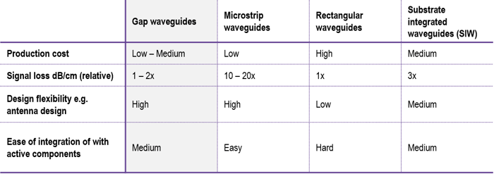 Figure 2. Comparison of gap waveguides and three alternative waveguide technologies
近日,電子科技大學自動化工程學院研究團隊在期刊《神經網絡》上發表研究性論文。該文首次提出毫米波近場透視成像與可見光的圖像融合方法。隨著目標檢測技術的快速發展,多種傳感器在提升檢測精度方面發揮著關鍵作用......
現代信息社會中,移動通信是實現信息高效流動的基本手段。近期,第五代移動通信系統(5G)已實現大規模商用。當前,5G長期演進和第六代移動通信系統(6G)成為學術界和產業界的研究熱點。實現高通量無線通信的......
毫米波(名詞解釋?)與太赫茲波(名詞解釋?)探測技術在通信、安全、生物檢測、頻譜分析等領域有著廣泛的應用。它們是將承載著毫米波與太赫茲波的光信息轉變為電信號的核心技術。高靈敏度、寬波段、快速響應及面陣......
近日,由中國科學院沈陽自動化研究所團隊與以色列魏茨曼科學院(WeizmannInstituteofScience)研究團隊,聯合提出了針對多輸入多輸出(Multiple-InputMultiple-O......
在時間某處,也許就是此刻新一代的技術變革正激發全新理念的誕生作為未來科技的推動者我們幫助從事前沿研究的高校、公司、研究機構,開啟測量新視野使其產品從概念到商用,速度更快科技的迅猛發展帶來了很多新的變化......
今日推薦文章作者為東南大學毫米波國家重點實驗室主任、IEEEFellow著名毫米波專家洪偉教授,本文選自《毫米波與太赫茲技術》,發表于《中國科學:信息科學》2016年第46卷第8期——《信息科學與技術......
對于投資者來說,軍民融合一直是雙創中一個重要的領域,由高校實驗室走出的項目往往具有高精尖等特點。但是另一方面,這些項目往往都是軍轉民,而且項目長期處于高校之中難以發現。為了提高科技成果轉化,支撐產業發......
由北京航空航天大學承擔的“新能源汽車”重點專項“電動汽車智能輔助駕駛關鍵技術研究與產品開發”項目“智能輔助駕駛環境感知關鍵技術研究與產品開發”課題研究取得階段性成果。課題重點圍繞77GHz毫米波雷達關......
分析測試百科網訊2017年2月23日,國家重大科學儀器設備開發專項“毫米波成像探測儀研制及產業化示范”項目(2012YQ140037)初步驗收會在同方威視密云基地召開。國家科技部資源配置司副司長吳學梯......
意大利電信近日宣布成立一個毫米波(mmWave)頻段實驗室,用于研究毫米波在5G網絡中的應用。意大利電信是歐洲第一家開設毫米波實驗室的電信運營商。這個位于都靈的實驗室包括遠場緊湊天線測試系統和球面近場......